
Printed Circuit Boards (PCBs) are used in almost every electronic device, from smartphones and computers to medical equipment, automotive systems and industrial machinery. These boards contain several small components, solder joints, connectors and electrical pathways that must be properly assembled to ensure the device works as expected.
Even a minor defect, such as a poorly soldered connection, damaged component or misplaced part, can affect the performance of an entire electronic assembly. This makes PCB inspection an important part of electronics manufacturing, repair and quality control.
Traditional visual inspection methods can make it difficult to examine very small components and identify defects accurately. This is where a digital microscope for PCB inspection becomes useful. It provides a magnified view of the circuit board on a screen, allowing technicians and quality inspectors to examine small details without depending entirely on conventional eyepiece microscopes.
With features such as high-resolution imaging, adjustable magnification, flexible lighting and image capture, digital microscopes make PCB inspection more convenient for everyday industrial applications.
What Is a Digital Microscope for PCB Inspection?
A digital microscope is an optical inspection device that uses a digital camera sensor to capture magnified images of an object and display them on a monitor or computer screen.
A digital microscope for PCB inspection is specifically used to examine printed circuit boards, electronic components, solder joints and other small areas that require close observation.
Unlike a conventional microscope, where the operator looks directly through eyepieces, a digital microscope displays the inspected area on a screen. This makes it easier to observe small details, adjust magnification and share inspection results with other team members.
Depending on the model, these systems may also offer features such as:
- High-resolution image and video output.
- Adjustable optical magnification.
- Automatic and manual focusing.
- LED lighting with brightness control.
- Image capture and video recording.
- Measurement and comparison functions.
- Different viewing angles for detailed inspection.
These features make digital microscopes useful in electronics manufacturing facilities, PCB assembly units, repair centres and quality inspection departments.
Why Is PCB Inspection Important in Electronics Manufacturing?
PCB inspection helps manufacturers identify assembly and component-related issues before the final electronic product reaches the customer.
During the manufacturing process, circuit boards pass through several stages, including solder paste application, component placement, soldering, cleaning and final testing. Problems can occur at any of these stages.
Some defects may be difficult to identify through normal visual checks, particularly when dealing with densely populated boards and small surface-mount components.
Common PCB defects include:
Soldering Defects
Solder joints establish electrical and mechanical connections between electronic components and the circuit board. Problems such as insufficient solder, excess solder, solder bridges and poor wetting can affect these connections.
A digital microscope helps inspectors examine solder joints closely and identify visible irregularities.
Component Misalignment
During PCB assembly, components must be positioned correctly according to the design specifications. Incorrect placement, tilted components or misaligned terminals can create assembly problems.
Magnified inspection makes it easier to examine component positioning and identify visible placement errors.
Damaged Components
Electronic components can develop cracks, chipped edges, damaged terminals or other physical defects during manufacturing, handling or transportation.
A microscope provides a closer view of these areas, helping inspectors identify visible damage.
PCB Surface Damage
Circuit boards may develop scratches, damaged solder pads, lifted tracks or other surface-related issues.
A digital inspection system helps technicians examine these areas before deciding whether repair or replacement is required.
How Does a Digital Microscope Help in PCB Inspection?
A digital microscope improves the way technicians examine small electronic components by providing a larger and clearer view of the inspection area.
Instead of relying on unaided vision, operators can examine specific sections of a PCB on a monitor and adjust the viewing settings according to the inspection requirement.
Here are some important ways a digital microscope supports PCB inspection.
Detailed Examination of Solder Joints
Solder joint inspection is one of the common applications of digital microscopes in electronics manufacturing.
Inspectors can examine individual solder connections to check for visible cracks, excess solder, bridging and other surface irregularities.
This is particularly useful when working with surface-mount components, where solder joints are often very small and closely spaced.
Inspection of Small Electronic Components
Modern PCBs contain resistors, capacitors, ICs, connectors and other components fitted into limited spaces.
A digital microscope allows operators to increase magnification and examine these components individually. This helps during assembly inspection, troubleshooting and repair work.
Examination of PCB Tracks and Pads
Copper tracks and solder pads play an important role in maintaining electrical connections across a circuit board.
A magnified view helps inspectors check for visible scratches, damaged pads, contamination and other surface issues that may require attention.
Better Visibility During PCB Repair
PCB repair often involves working with small components and closely spaced soldering points.
A digital microscope displays the work area on a monitor, allowing technicians to observe the component while carrying out inspection and precision repair activities.
Depending on its working distance and configuration, the system can also provide sufficient room for certain manual operations.
Important Features to Look for in a Digital Microscope for PCB Inspection
Choosing a digital microscope requires more than checking its maximum magnification. The system should match the type of components, inspection requirements and working conditions.
Some important features to consider include:
Magnification Range
Magnification determines how closely an operator can examine a component.
A suitable magnification range should allow both general observation of the PCB and detailed examination of smaller areas.
However, higher magnification alone does not guarantee better inspection. Image clarity, lens quality, resolution and field of view also matter.
High-Resolution Imaging
Image resolution affects how clearly small details appear on the monitor.
A high-resolution digital microscope helps inspectors examine solder joints, component edges and surface conditions with greater clarity.
For regular PCB inspection, Full HD imaging can be a useful option, depending on the level of detail required.
Adjustable Lighting
PCB surfaces, solder joints and metallic components can reflect light, making certain areas difficult to inspect.
Adjustable LED lighting allows operators to control brightness according to the material and inspection conditions.
Proper illumination helps reduce unwanted reflections and improves visibility across different parts of the board.
Working Distance
Working distance refers to the space between the microscope lens and the object being inspected.
This is particularly important during PCB repair and rework because technicians may need additional space for soldering tools, probes or other equipment.
A suitable working distance makes the inspection process more practical without compromising visibility.
Image Capture and Measurement
Some digital microscopes support image capture, video recording and measurement functions.
These features can help quality control teams maintain inspection records, compare components and document visible defects.
Measurement capabilities are useful when the microscope and its software support the required calibration and measurement accuracy.
Viewing Angle and Focus Control
A fixed top-view image may not provide enough information when inspecting connectors, raised components or side-mounted solder joints.
Microscopes with flexible viewing arrangements allow operators to examine different areas from more suitable angles.
Automatic and manual focusing options can also make repeated inspection tasks easier.
Applications of Digital Microscopes in the Electronics Industry
Digital microscopes are used in several areas where small components and fine details need to be examined.
PCB Assembly Inspection
During PCB assembly, inspectors check component placement, soldering conditions and visible surface defects. A digital microscope provides magnified images that help identify issues before the board moves to the next production stage.
SMT Component Inspection
Surface Mount Technology (SMT) involves placing electronic components directly onto the surface of a PCB. Since SMT components are often small and closely arranged, detailed inspection is important. Digital microscopes help examine component alignment, solder joints, terminal conditions and other visible assembly details.
PCB Rework and Repair
During rework, technicians may need to remove, replace or repair individual components without affecting nearby connections. A digital microscope helps them observe the working area more closely and identify the exact location of a visible defect.
Quality Control Departments
Quality control teams inspect circuit boards to ensure that visible assembly and component conditions meet the required standards. Digital microscopes can support these checks by providing magnified images that are easier to observe and document.
Research and Development
Electronic product development often involves testing different circuit layouts, components and assembly methods. Digital microscopes help engineers examine prototypes, investigate visible defects and study small electronic structures during development work.
Digital Microscope vs Traditional Microscope for PCB Inspection
Both digital and traditional microscopes are used for close inspection, but their viewing methods and working features are different.
| Feature | Digital Microscope | Traditional Microscope |
| Viewing | Monitor or screen | Eyepiece |
| Image capture | Available in supported models | Requires additional equipment |
| Image sharing | Easier through digital output | Less convenient |
| Measurement | Available with compatible software | Depends on accessories |
| Viewing comfort | Screen-based observation | Direct eyepiece observation |
| Group inspection | Multiple people can view the screen | Generally individual viewing |
A digital microscope is particularly useful when inspection involves image documentation, screen-based observation or collaboration between team members.
A traditional microscope may still be suitable for applications where direct optical viewing is preferred.
The right choice depends on the inspection process, budget and technical requirements.
How to Choose the Right Digital Microscope for PCB Inspection?
Before purchasing a digital microscope, businesses should understand their inspection requirements.
A microscope used for checking larger PCB assemblies may have different requirements from one used for examining fine-pitch components or carrying out detailed rework.
Consider the following points before selecting a system:
- Identify the Inspection Requirement: Determine whether the microscope will be used for general PCB inspection, solder joint examination, component checking or precision repair.
- Check Magnification and Resolution: Select a system that provides sufficient magnification without compromising image clarity.
- Consider Working Distance: Make sure there is enough space between the lens and the PCB for the intended inspection or repair work.
- Evaluate Lighting Options: Adjustable illumination is useful when inspecting reflective solder joints and different PCB surfaces.
- Check Image Output: Consider whether HDMI, USB or other output options are required for connecting the microscope to a monitor or computer.
- Look at Additional Functions: Features such as autofocus, image capture, measurement and flexible viewing angles can be useful depending on the application.
- Consider After-Sales Support: Industrial inspection equipment should be supported by reliable technical assistance to help with installation, operation and maintenance.
Digital Microscope Solutions Available at Sumitron
For electronics manufacturers, repair teams and quality inspection departments, selecting the right optical inspection equipment is an important part of maintaining consistent inspection practices.
Sumitron offers digital microscope and video inspection solutions through its optical inspection systems range.
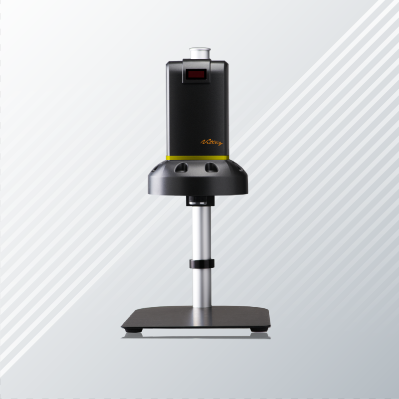
One of the relevant options is the UM08D-CSZ064 DIGI Microscope, designed for detailed inspection of electronic components, soldering points and precision parts.
Some of its key features include:
- Magnification range of 22x–147x on a 24-inch monitor.
- 2-megapixel CMOS sensor.
- Full HD 1080P video output at 60 fps.
- Top-view and side-view inspection.
- 2D and 3D observation capabilities.
- 360-degree inspection.
- Adjustable LED ring lighting.
- Manual observation-angle adjustment.
The ability to examine components from different directions makes this microscope particularly useful for applications where a top-view inspection alone may not provide sufficient information.
Apart from this model, Sumitron offers other ViTiny digital microscope options, including UM08B, UM30, UM20 and UM12 USB Auto Focus Digital Microscope.
The selection of a particular model should depend on the inspection area, required magnification, working distance and other application-specific needs.
Frequently Asked Questions
Q1. What is a digital microscope used for in PCB inspection?
Ans. A digital microscope is used to examine printed circuit boards, solder joints, electronic components and PCB tracks at higher magnification. It helps inspectors identify visible defects that may be difficult to notice through normal visual inspection.
Q2. Why is a digital microscope important for electronics manufacturing?
Ans. It provides a magnified view of small components and connections, helping technicians examine assembly quality, identify visible defects and carry out detailed inspection during manufacturing and repair.
Q3. Can a digital microscope detect soldering defects on PCBs?
Ans. Yes. A digital microscope helps inspect solder joints for visible problems such as solder bridges, insufficient solder, cracks and irregular solder surfaces. However, defects hidden beneath components may require additional inspection methods.
Q4. What magnification is required for PCB inspection?
Ans. The required magnification depends on the size of the components and the level of detail needed. A microscope with an adjustable magnification range is useful because it allows operators to switch between general PCB observation and close component inspection.
Q5. What is the difference between a digital microscope and a USB microscope?
Ans. A USB microscope generally connects to a computer through a USB interface and displays images using compatible software. Digital inspection systems may offer additional features such as HDMI output, advanced focusing, adjustable lighting, measurement and specialised optical arrangements.
Q6. Can digital microscopes be used for SMT inspection?
Ans. Yes. Digital microscopes are useful for examining SMT components, solder joints, component alignment and other visible details during PCB assembly and quality inspection.
Q7. What features should I check before buying a PCB inspection microscope?
Ans. Important features include magnification range, image resolution, working distance, lighting adjustment, focusing options, viewing angles, image output and measurement capabilities.
Q8. Can a digital microscope be used for PCB repair and rework?
Ans. Yes. It helps technicians observe small soldering points, electronic components and damaged areas while performing inspection and repair work. The working distance should be suitable for the tools being used.
Q9. What is the UM08D-CSZ064 DIGI Microscope used for?
Ans. The UM08D-CSZ064 is used for detailed inspection of PCBs, solder joints, electronic components and precision parts. It supports 2D and 3D observation, top-view and side-view inspection, and 360-degree viewing.
Conclusion
PCB inspection is an important part of electronics manufacturing because even small assembly defects can affect the performance and reliability of an electronic device.
A digital microscope for PCB inspection gives technicians and quality inspectors a closer view of solder joints, electronic components, PCB tracks and other small areas that may be difficult to examine through normal visual checks.
Features such as high-resolution imaging, adjustable magnification, controlled lighting, image capture and flexible viewing angles make digital microscopes useful for PCB assembly, SMT inspection, repair and quality control.
For businesses looking for suitable optical inspection equipment, Sumitron offers digital microscope solutions designed for different industrial inspection requirements.
Selecting the right system based on the actual application can help inspection teams examine components more effectively and make better-informed quality control decisions.
For more information about digital microscopes and optical inspection systems, visit Sumitron or contact its team to discuss your inspection requirements.
Read Also This Blog


[…] Digital Microscope for PCB Inspection: Features, Uses and Benefits […]